

Which Semiconductor Material Risks Should Sourcing Teams Assess?
Which Semiconductor Material Risks Should Sourcing Teams Assess?
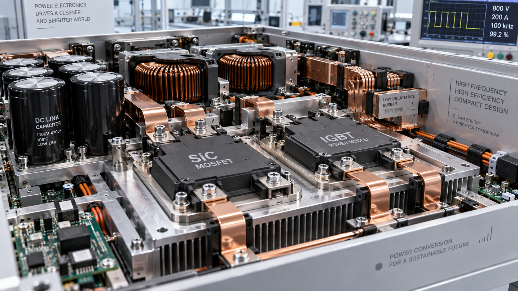
Which semiconductor material risks should be included in sourcing? For procurement teams supporting power electronics, advanced packaging, and industrial sensors, the answer extends beyond price and availability. Purity deviations, SiC crystal defects, inconsistent GaN epitaxial structures, and contamination in electronic chemicals can undermine yield, reliability, and qualification timelines. Supplier concentration, export restrictions, and weak lot-level traceability add further exposure.
The practical challenge is deciding which variations matter to a particular manufacturing process. A material can satisfy its supplier’s specification yet remain unsuitable for the buyer’s process window. Conversely, demanding the tightest available specification on every parameter can increase cost without improving performance. Good sourcing connects material characteristics to measurable manufacturing and field risks.
G-SSI’s technical benchmarking focus spans power semiconductors, advanced packaging, industrial sensors, electronic chemicals, and fabrication environments. That cross-functional view is useful here: procurement cannot assess a wafer, encapsulant, or specialty gas independently of the process that consumes it.
Start with the failure consequence, not the material grade
A sourcing risk register should distinguish between a production interruption, a recoverable yield loss, and a latent reliability defect. These consequences require different controls. An incoming inspection may detect wafer breakage; it will not necessarily reveal a packaging material that develops adhesion problems after thermal cycling.
Ask process engineering and reliability teams to identify the characteristics that influence each failure mechanism. For a power device, these may include substrate defects, epitaxial uniformity, or contamination affecting gate dielectric integrity. For a MEMS sensor, package stress, outgassing, and cavity cleanliness may influence offset or long-term drift.
Then rank risks using severity, likelihood, detectability, and recovery time. A low-volume material with no qualified replacement can deserve more attention than a high-spend commodity. The purchasing value is not a reliable proxy for operational exposure.
Purity claims need impurity-specific evidence
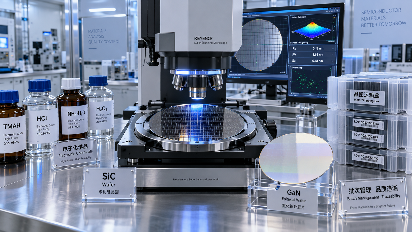
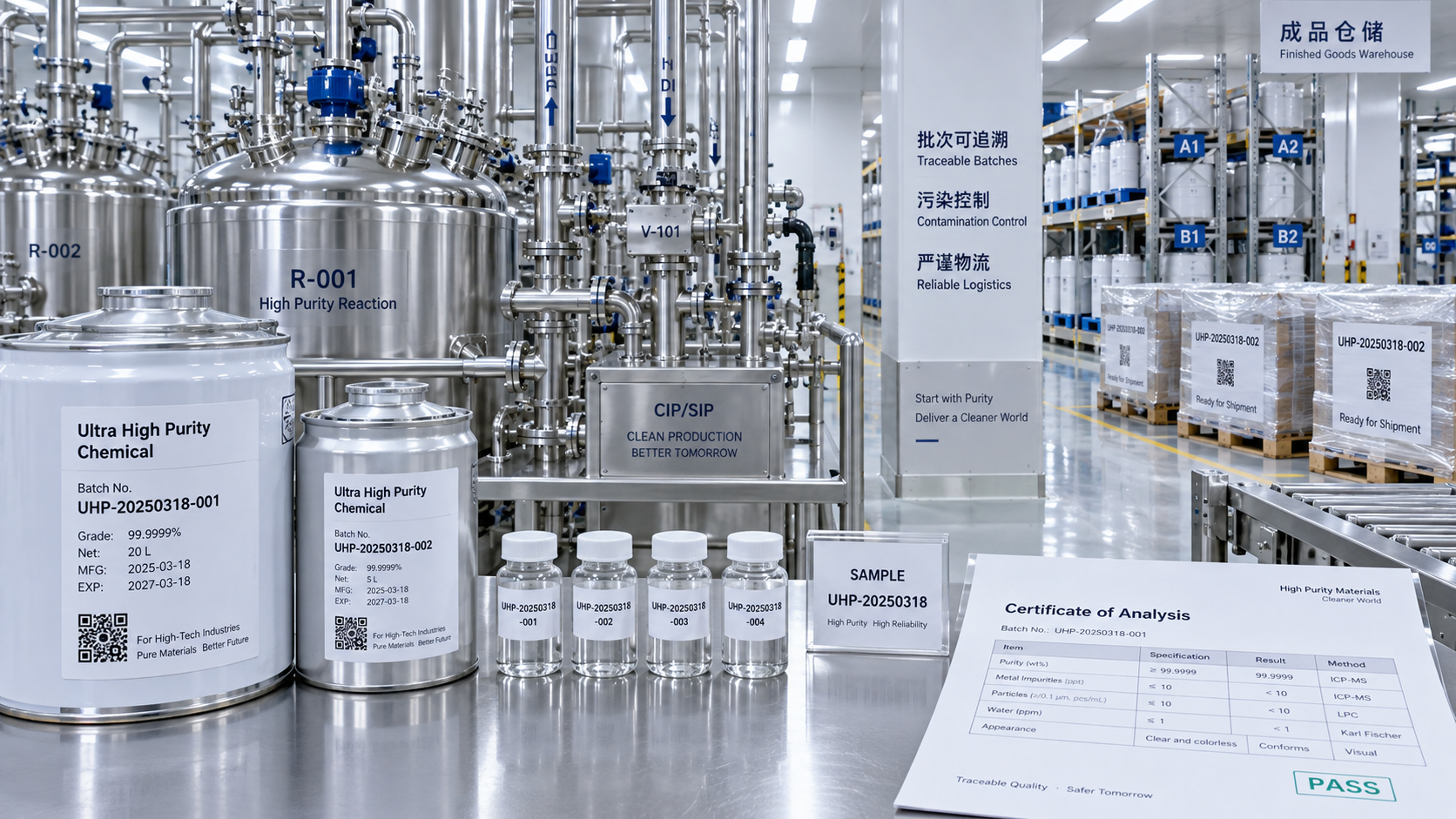
“Semiconductor grade” is not a complete purchasing specification. For wet chemicals and specialty gases, the relevant questions concern individual contaminants, analytical sensitivity, sampling conditions, and stability through delivery. A high headline purity does not establish that moisture, oxygen, metals, particles, or organic residues meet the process requirement.
Request limits for critical impurities rather than relying only on total purity. The supplier’s analytical method must resolve those limits with appropriate detection capability and uncertainty. “Not detected” means little without the detection limit; it does not mean that a contaminant is absent.
The certificate of analysis also needs interpretation. Does it report measurements from the delivered lot, a representative production batch, or periodic verification? Which properties are tested on every lot, and which are guaranteed through process controls? Those distinctions should be explicit before purchase approval.
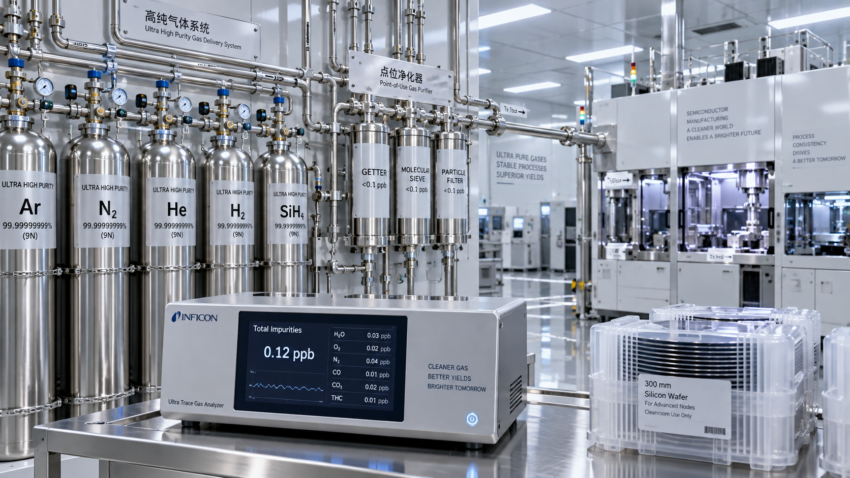
Container preparation, cylinder valves, transfer lines, filtration, and storage can compromise material after release. For sensitive processes, point-of-use verification may be necessary. Sub-ppb purity claims should therefore be evaluated alongside the sampling and delivery system, not treated as an isolated quality promise.
SiC and GaN require more than a dimensional check
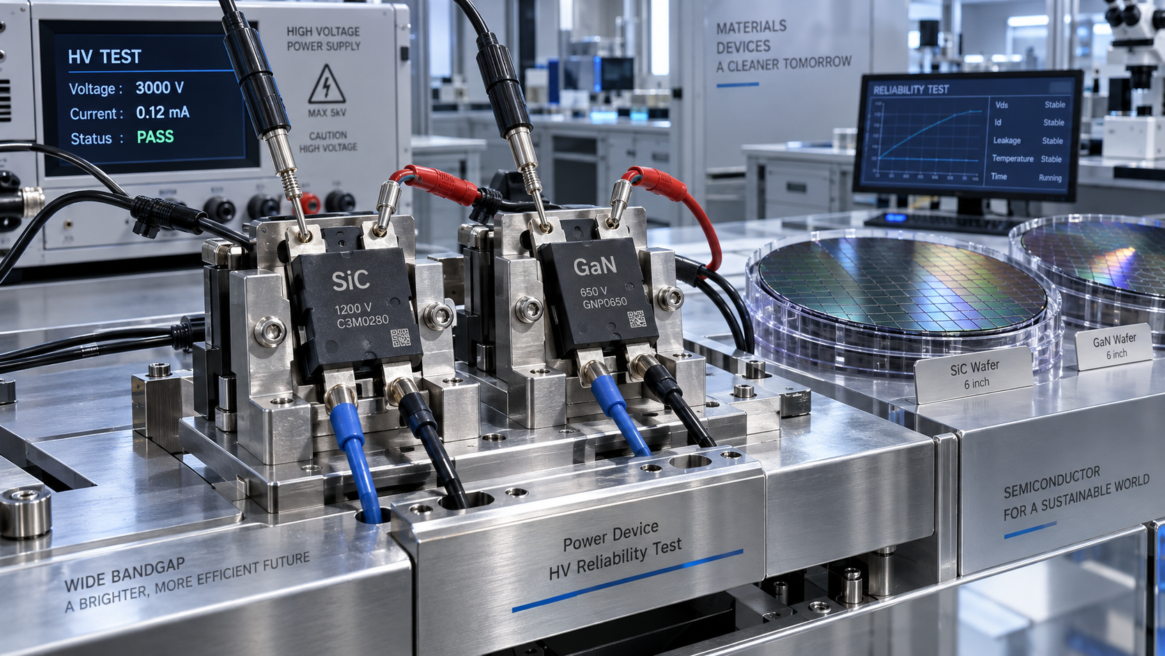
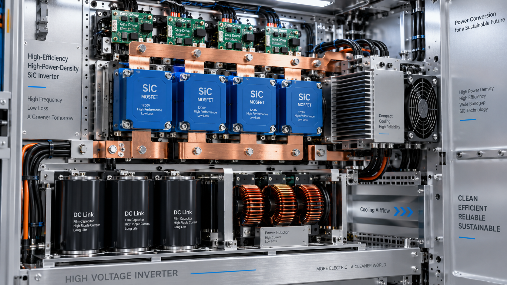
For silicon carbide, assess substrate and epitaxial material separately. Wafer diameter, thickness, orientation, resistivity, bow, warp, and surface condition matter, but they do not capture the full defect landscape. Micropipes, dislocations, stacking faults, and epitaxial defects can have different implications depending on the device structure and operating conditions.
Basal plane dislocations deserve particular attention where bipolar conduction may contribute to stacking-fault expansion. However, a sourcing team should not translate a single defect metric directly into a universal field-failure prediction. Device design, epitaxial processing, and qualification results must inform the acceptance limit.
For GaN, clarify exactly what is being sourced. Bulk GaN, GaN-on-silicon, and GaN-on-SiC are not interchangeable material categories. Substrate choice and epitaxial stack affect thermal behavior, stress, wafer handling, and device processing. Relevant evidence may include layer thickness and composition uniformity, defect characterization, buffer leakage, and wafer bow after growth.
Mapping data often reveals more than wafer averages. Edge exclusions and localized defects can change usable die yield even when average values look acceptable. Agree on inspection coverage, defect classification, and map format so supplier and buyer are comparing the same population.
Packaging and sensor materials can pass incoming checks and still fail later
Advanced packaging adds interfaces where material compatibility becomes a reliability issue. Mold compounds, underfills, die-attach materials, redistribution dielectrics, and package substrates should be evaluated as part of an assembly, not only as individual products. Thermal expansion mismatch, moisture absorption, ionic contamination, cure behavior, and adhesion can affect delamination, warpage, corrosion, or interconnect fatigue.
In 2.5D and 3D assemblies, dimensional stability and interface behavior become especially important because multiple dies and interconnect structures must remain aligned and mechanically compatible. A supplier’s datasheet value for thermal conductivity or glass transition temperature cannot substitute for validation under the intended assembly process.
Industrial MEMS adds a different sensitivity: a material change may alter measurement performance without causing an obvious electrical failure. Adhesive shrinkage, package stress, volatile residues, or seal changes can influence calibration and drift. Qualification should therefore include relevant sensor outputs after environmental exposure, not merely continuity checks.
This is where procurement needs an explicit change-control agreement. Changes to formulation, raw-material source, manufacturing site, cure recommendations, or packaging require review when they can affect qualified performance—even if the commercial part number remains unchanged.
Traceability must survive repacking, transport, and process changes
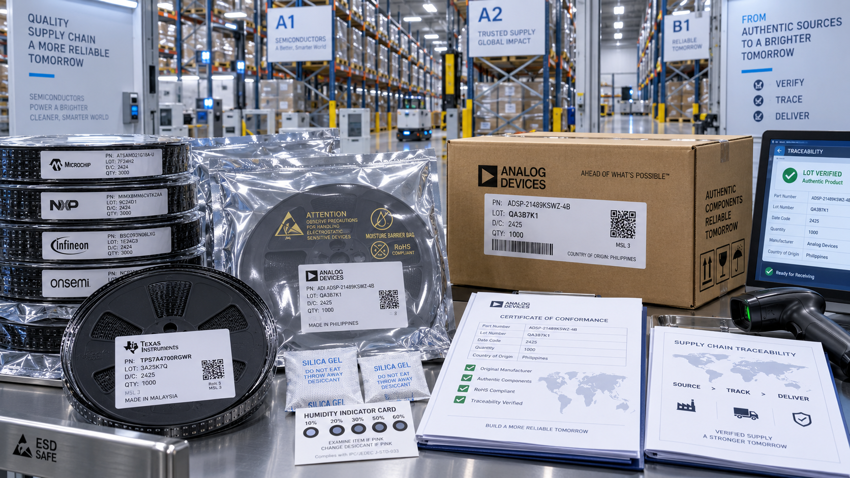
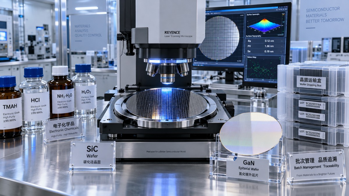
A lot number is useful only if it connects the delivered material to meaningful records. Depending on the material, that chain may include crystal growth, epitaxy, chemical production, purification, filling, inspection, and shipment. Distributors and repackers can introduce gaps unless record transfer is contractually defined.
The objective is not paperwork volume. It is the ability to isolate affected inventory, investigate excursions, and determine whether neighboring lots share the same exposure. Procurement should confirm how quickly records can be retrieved and whether retained samples are available where appropriate.
- Define which production and test records must accompany or remain linked to each shipment.
- Specify storage conditions, shelf life, and transport controls for moisture-sensitive or temperature-sensitive materials.
- Require advance notification and approval rules for changes affecting qualified characteristics.
- Establish containment, replacement, and investigation responsibilities for nonconforming lots.
Environmental control belongs in this assessment too. Cleanroom conditions, handling procedures, packaging cleanliness, and exposure during transfer can change the material reaching the tool. Supplier approval and internal handling controls need to meet at a clearly defined acceptance point.
Supply continuity is a technical qualification problem
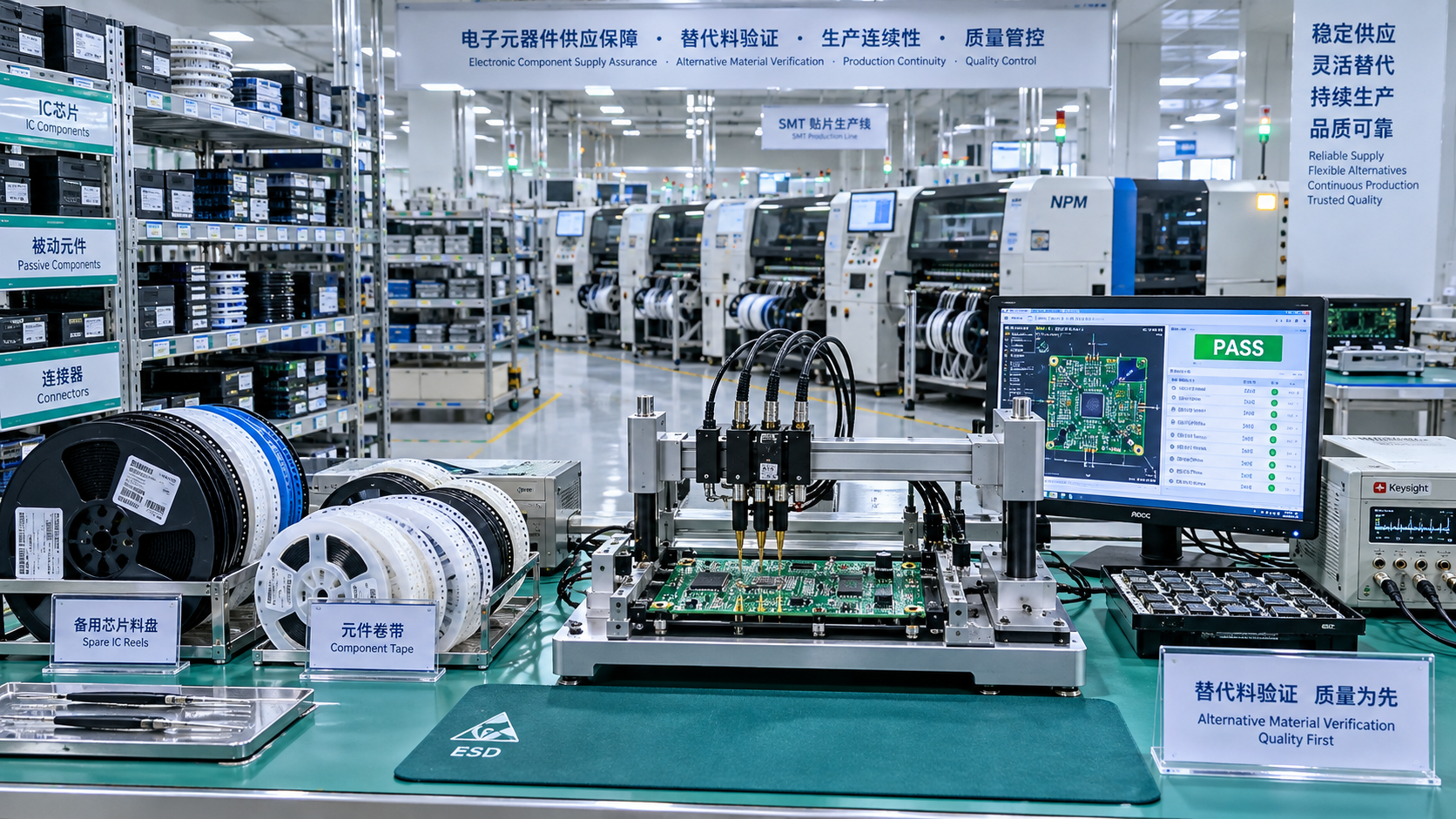
Two approved vendors do not necessarily provide two independent supply chains. They may share a substrate producer, precursor manufacturer, purification facility, or logistics route. Assess upstream dependencies where commercially accessible, particularly for materials with specialized production equipment or lengthy qualification cycles.
Alternative sourcing also needs a realistic conversion plan. Different wafer characteristics can require process tuning; a replacement underfill may require assembly and reliability validation. Nominally equivalent grades should not be counted as interchangeable until the relevant engineering work is complete.
Capacity expansion does not automatically provide qualified capacity. For mature-node supply from China or any other manufacturing region, verify the actual production site, material source, process controls, and evidence supporting the intended application. Geographic labels are neither a qualification nor a disqualification.
Export controls, customs requirements, hazardous-material transport rules, and end-use restrictions require transaction-specific review. Applicability depends on the material, origin, destination, parties, and current rules. Do not assume that a previous shipment establishes future eligibility.
Inventory buffers must also account for usable shelf life and requalification needs. Stock that expires before consumption is not effective continuity protection. Compare buffer stock, reserved capacity, and qualified alternatives against the likely duration and consequence of disruption.
Use standards correctly—and close the evidence gaps
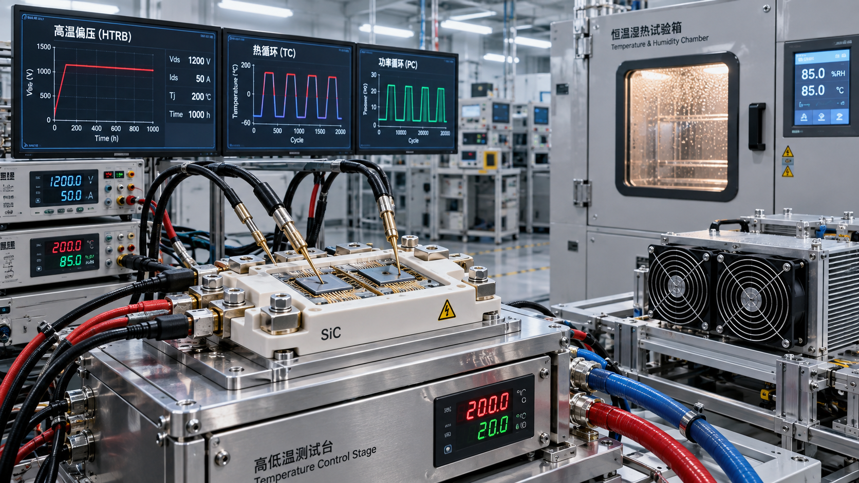
Standards provide a common language, but their scope matters. Applicable SEMI documents can support material specifications, test methods, and handling requirements. AEC-Q100 concerns stress-test qualification for integrated circuits; it is not a blanket certification for raw materials. Automotive discrete semiconductor applications may call for AEC-Q101 instead, depending on the device and customer requirements.
ISO/IEC 17025 accreditation supports laboratory competence for activities within the accredited scope. It does not certify every material tested by that laboratory. Check whether the relevant method, analyte, and measurement range are covered, and confirm which standard revision the contract invokes.
G-SSI’s benchmarking approach is most useful when it connects these requirements across materials, devices, packaging, and fabrication conditions. The output should be a project-specific evidence set—not an unsupported assertion that a supplier meets “international standards.”
Before award, give each critical material an acceptance limit, a verification method, an accountable owner, and a response plan for excursions. Where evidence is incomplete, distinguish between a limited engineering trial and unrestricted production approval. The decisive question is whether the team can detect unacceptable variation before it reaches production—or contain it quickly if it does.
Get weekly intelligence in your inbox.
No noise. No sponsored content. Pure intelligence.
 Apr 28, 2026When do rapid prototyping 3D printing services save real costWhen do rapid prototyping 3D printing services save real cost
 Apr 28, 2026What Can Go Wrong in Fan-out Wafer Level Pkg?What Can Go Wrong in Fan-out Wafer Level Pkg?
 Apr 28, 2026What Makes Optical LiDAR Modules Better for Autonomy?What Makes Optical LiDAR Modules Better for Autonomy?
 Apr 28, 20262026 Market Trends in Supply Chain Resilience for Fabs2026 Market Trends in Supply Chain Resilience for Fabs
 Oct 14, 2026How third-generation semiconductors achieve high breakdown voltagesHow third-generation semiconductors achieve high breakdown voltages
 Oct 13, 2026When does parallel testing cut high-volume semiconductor testing costs?When does parallel testing cut high-volume semiconductor testing costs?
 Oct 12, 2026Preventing Electronics Production Stoppages from Component ShortagesPreventing Electronics Production Stoppages from Component Shortages
 Oct 12, 2026Electronics Supply Chain Resilience: When to Dual-Source or Hold Safety StockElectronics Supply Chain Resilience: When to Dual-Source or Hold Safety Stock
 Oct 12, 2026Which Semiconductor Material Risks Should Sourcing Teams Assess?Which Semiconductor Material Risks Should Sourcing Teams Assess?
 Oct 12, 2026What Should You Check Before Switching KrF/ArF Photoresist Suppliers?What Should You Check Before Switching KrF/ArF Photoresist Suppliers?
 Oct 12, 2026When does fan-out wafer level packaging outperform flip-chip packaging?When does fan-out wafer level packaging outperform flip-chip packaging?
 Oct 11, 2026How energy management can reduce peak demand chargesHow energy management can reduce peak demand charges
 Oct 10, 2026When do integrated sensor systems reduce commissioning risks?When do integrated sensor systems reduce commissioning risks?
 Oct 09, 2026How North American semiconductor fabs control airborne molecular contaminationHow North American semiconductor fabs control airborne molecular contamination
 Oct 08, 2026When do custom aluminum extrusions reduce fabrication costs?When do custom aluminum extrusions reduce fabrication costs?
 Oct 07, 2026How semiconductor packaging affects thermal reliability in EV power electronicsHow semiconductor packaging affects thermal reliability in EV power electronics
 Oct 06, 2026When do corrugated plastic boxes make sense for returnable shipping?When do corrugated plastic boxes make sense for returnable shipping?
 Oct 05, 2026What to verify before choosing semiconductor distributors in North AmericaWhat to verify before choosing semiconductor distributors in North America
 Oct 04, 2026How to assess a high purity materials manufacturer’s traceabilityHow to assess a high purity materials manufacturer’s traceability
 Oct 03, 2026How SiC power conversion solutions improve high-voltage invertersHow SiC power conversion solutions improve high-voltage inverters
 Oct 02, 2026When do SiC MOSFET benefits justify the higher device cost?When do SiC MOSFET benefits justify the higher device cost?
 Oct 01, 2026Which semiconductor reliability testing standards apply to power devices?Which semiconductor reliability testing standards apply to power devices?
 Sep 30, 2026How to qualify a semiconductor photoresist supplier for KrF/ArF productionHow to qualify a semiconductor photoresist supplier for KrF/ArF production
 Sep 29, 2026What image quality should portable ultrasound scanners deliver for triage?What image quality should portable ultrasound scanners deliver for triage?
 Sep 28, 2026How sub-ppb impurity control gases protect process consistencyHow sub-ppb impurity control gases protect process consistency
 Sep 27, 2026How chemical purity affects defect rates in semiconductor depositionHow chemical purity affects defect rates in semiconductor deposition
 Sep 26, 2026When do high voltage power semiconductor devices need SiC over IGBTs?When do high voltage power semiconductor devices need SiC over IGBTs?