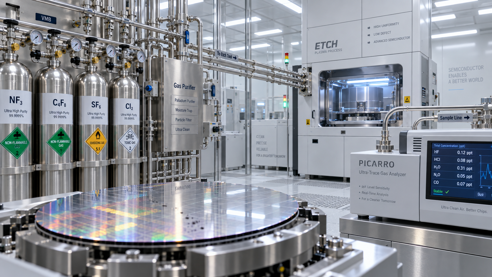


Semiconductor Environmental Control Cost Pitfalls
Semiconductor Environmental Control costs often appear manageable on paper, yet hidden design flaws, energy inefficiencies, contamination risks, and compliance gaps can quietly erode ROI. For financial approvers, understanding these cost pitfalls is essential to balancing capital discipline with fab reliability, yield protection, and long-term operational resilience in an increasingly demanding semiconductor landscape.
Why Semiconductor Environmental Control Becomes a Financial Risk Faster Than Expected
For finance leaders, Semiconductor Environmental Control is rarely just a facilities expense. It directly affects wafer yield, tool uptime, contamination rates, utility volatility, audit readiness, and expansion flexibility.
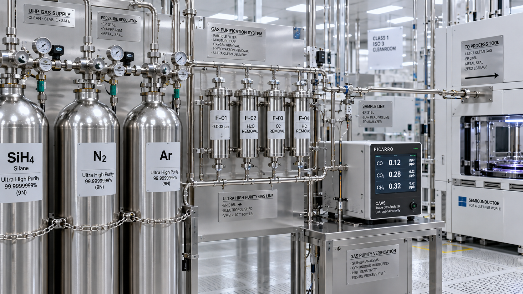
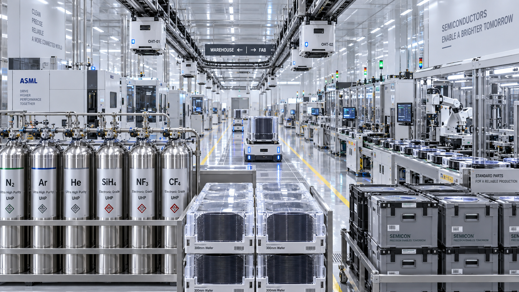
In fabs, packaging lines, sensor manufacturing, and high-purity chemical handling areas, environmental control covers temperature, humidity, airborne particles, vibration, pressure cascade, exhaust integrity, and gas purity support conditions.
When these elements are underdesigned, the damage is rarely immediate and obvious. Instead, costs accumulate through scrap, retest, requalification, emergency maintenance, higher energy demand, and delayed customer approvals.
- Capital budgets often focus on equipment purchase price while underestimating lifecycle costs from HVAC loads, filtration replacement, monitoring calibration, and cleanroom balancing.
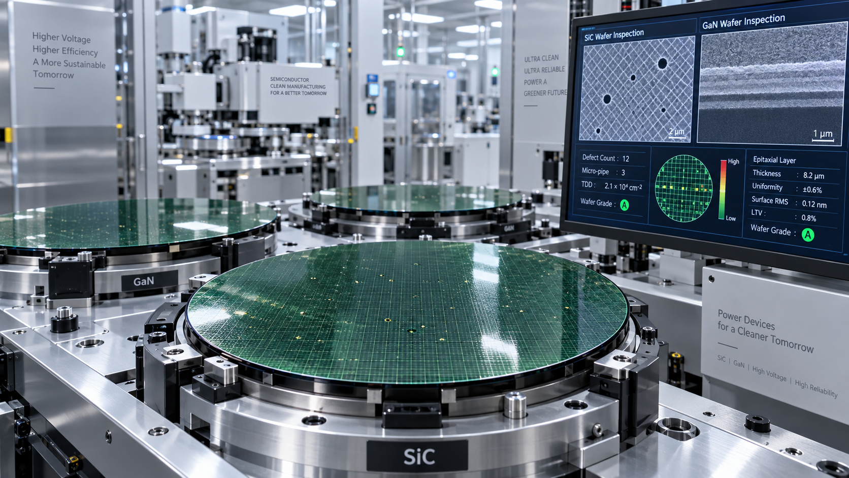
- Operational teams may specify performance margins that are too broad for advanced packaging, MEMS, SiC, GaN, or specialty gas environments.
- Compliance gaps can trigger indirect financial losses when customer audits identify weak environmental traceability or insufficient monitoring records.
Why hidden costs matter to approval teams
Approval teams are judged on budget discipline, but they also carry the downside of approving systems that later force expensive retrofits. In Semiconductor Environmental Control, the cheapest initial proposal is often the most expensive operational outcome.
Which Cost Pitfalls Appear Most Often in Semiconductor Environmental Control Projects?
The most common pitfalls are not exotic technical failures. They are familiar procurement mistakes: incomplete scope definition, weak performance baselines, and poor alignment between process risk and facility design.
The table below helps financial approvers identify where Semiconductor Environmental Control spending tends to deviate from initial assumptions and how those deviations affect long-term economics.
These pitfalls show why Semiconductor Environmental Control should be reviewed as a risk-adjusted investment. For financial approvers, the right question is not “What is the lowest bid?” but “What cost exposure does each design leave behind?”
The hidden retrofit problem
Retrofits inside operating semiconductor environments are especially costly. Shutdown windows are narrow, contamination controls are stricter, and changes can require requalification. A small upfront saving may later trigger a disproportionately large correction budget.
How Financial Approvers Should Compare Semiconductor Environmental Control Options
A practical comparison must go beyond capex. Financial approvers need to evaluate operating burden, process fit, maintenance dependency, and audit defensibility. This is especially important when multiple departments submit different technical assumptions.
The following comparison framework can help standardize discussions between finance, facilities, process engineering, quality, and procurement.
This comparison makes one point clear: Semiconductor Environmental Control should be purchased as operational infrastructure, not as a commodity package. Finance teams that adopt a lifecycle lens usually reduce surprise spending later.
Questions worth asking before approval
- What process-sensitive zones require tighter particle, humidity, pressure, or vibration control than the general facility?
- What are the expected annual maintenance and filter replacement costs under real operating conditions?
- How quickly can the system recover from process door openings, tool heat spikes, or utility disturbances?
- What documentation supports SEMI-related customer requirements, calibration control, and environmental data retention?
What Technical and Compliance Factors Drive Total Cost?
Many Semiconductor Environmental Control budgets fail because technical parameters are treated as engineering detail rather than financial drivers. In reality, parameter accuracy shapes both process consistency and future remediation costs.
Key technical factors
- Temperature stability affects lithography support areas, test environments, packaging reliability, and metrology repeatability.
- Humidity control influences electrostatic behavior, moisture sensitivity, chemical handling conditions, and storage integrity for sensitive materials.
- Pressure differentials protect critical rooms from cross-contamination and determine whether airflow moves in the intended direction.
- Particle and molecular contamination management is central to yield, especially in advanced packaging, MEMS, and high-purity chemical interfaces.
- Monitoring granularity determines whether excursions are detected early or only after product defects appear downstream.
Relevant standards and governance context
Depending on the application, financial approvers may encounter references to SEMI practices, ISO cleanroom principles, ISO/IEC 17025 calibration expectations, and customer-specific quality controls. These are not paperwork burdens alone.
They influence what must be monitored, recorded, validated, and maintained. If compliance expectations are overlooked during approval, later corrective work can affect both project timing and customer confidence.
Where Do Different Semiconductor Scenarios Require Different Control Budgets?
Not every facility requires the same Semiconductor Environmental Control profile. Cost discipline improves when the control level matches the actual contamination sensitivity, thermal load, and process dependency of each zone.
The scenario table below helps finance and procurement teams connect environmental specifications with business use cases instead of applying one uniform budget assumption.
For diversified industrial groups, this scenario-based budgeting approach is more effective than applying a single environmental standard across all operations. It protects capital while preserving process-critical performance where it matters most.
How G-SSI Supports Better Approval Decisions
G-SSI is positioned at the intersection of technical benchmarking, supply chain resilience, and semiconductor operating reality. That matters because financial approvers often receive fragmented input from engineering, facilities, vendors, and quality teams.
By connecting Semiconductor Environmental Control with broader silicon value chain requirements, G-SSI helps decision-makers evaluate environmental infrastructure in the same framework as packaging reliability, power device integrity, sensor precision, and high-purity material handling.
Where this becomes valuable
- When a project must reconcile China-based expansion speed with internationally accepted reliability and documentation expectations.
- When mature-node production economics require strict capex control without compromising contamination protection and thermal stability.
- When corporate groups need one benchmark language across SiC, GaN, advanced packaging, MEMS, and specialty gas related environments.
This benchmarking role is especially useful for finance teams that need a neutral basis for reviewing technical claims. It reduces the chance that a decision depends only on the most persuasive vendor narrative.
FAQ: What Financial Approvers Ask About Semiconductor Environmental Control
How should Semiconductor Environmental Control be evaluated beyond capex?
Use a lifecycle model that includes utilities, preventive maintenance, calibration, filters, downtime exposure, qualification support, and retrofit probability. This gives a more realistic approval basis than purchase price alone.
What is the most common budgeting mistake?
The most common mistake is assuming general industrial HVAC logic is enough for semiconductor spaces. Semiconductor Environmental Control requires tighter zoning, better monitoring, and stronger contamination logic than conventional manufacturing environments.
Which projects are most exposed to hidden environmental control costs?
Projects involving advanced packaging, MEMS, precision test, electronic chemical support, and capacity expansion in existing facilities tend to face the greatest hidden costs because process sensitivity and retrofit constraints are higher.
What should be confirmed before budget release?
Confirm zone-by-zone performance targets, monitoring architecture, maintenance assumptions, utility model boundaries, compliance documentation scope, and commissioning responsibilities. These items strongly influence future cost stability.
Why Many Strong Business Cases Still Fail During Implementation
Even a sound budget can fail if implementation governance is weak. Semiconductor Environmental Control projects often cross facilities engineering, EHS, process ownership, quality assurance, and procurement. If responsibilities are vague, scope drift follows.
- Commissioning criteria are not linked to process acceptance, so a technically installed system may still be operationally unfit.
- Data logging and calibration ownership are assigned too late, weakening traceability from the first day of operation.
- Expansion allowances are omitted, causing future production increases to overload the original environmental design.
For financial approvers, these implementation details are not minor operational concerns. They determine whether the approved asset delivers the expected return or becomes a recurring exception request.
Why Choose Us for Semiconductor Environmental Control Decision Support
If your team is evaluating Semiconductor Environmental Control for wafer fabs, advanced packaging, MEMS, smart sensor lines, or high-purity chemical and gas support areas, G-SSI can help structure the decision before hidden costs are locked in.
Our support focus is practical and decision-oriented. We can help you review control parameters, compare technical options, align facility assumptions with process sensitivity, and clarify the documentation needed for internal approval or external customer review.
- Confirm key parameters such as cleanliness logic, humidity precision, pressure zoning, temperature stability, and monitoring depth.
- Discuss solution selection for different operating scenarios, from mature-node fabrication to advanced packaging and sensor manufacturing.
- Review delivery timing assumptions, commissioning dependencies, and likely retrofit risks before final approval.
- Explore custom benchmarking needs tied to SEMI-related expectations, ISO/IEC 17025 calibration context, or customer audit preparation.
- Open a targeted quotation discussion based on lifecycle cost logic instead of price-only comparisons.
For financial approvers, the value of Semiconductor Environmental Control is not found in specification sheets alone. It is found in fewer surprises, stronger yield protection, more credible budgeting, and infrastructure that supports long-term semiconductor competitiveness. Contact G-SSI to review your parameter assumptions, selection path, certification concerns, implementation risks, and budget justification framework before the next approval milestone.
Get weekly intelligence in your inbox.
No noise. No sponsored content. Pure intelligence.
 Apr 28, 2026When do rapid prototyping 3D printing services save real costWhen do rapid prototyping 3D printing services save real cost
 Apr 28, 2026What Can Go Wrong in Fan-out Wafer Level Pkg?What Can Go Wrong in Fan-out Wafer Level Pkg?
 Apr 28, 2026What Makes Optical LiDAR Modules Better for Autonomy?What Makes Optical LiDAR Modules Better for Autonomy?
 Apr 28, 20262026 Market Trends in Supply Chain Resilience for Fabs2026 Market Trends in Supply Chain Resilience for Fabs
 Oct 10, 2026When do integrated sensor systems reduce commissioning risks?When do integrated sensor systems reduce commissioning risks?
 Oct 09, 2026How North American semiconductor fabs control airborne molecular contaminationHow North American semiconductor fabs control airborne molecular contamination
 Oct 08, 2026When do custom aluminum extrusions reduce fabrication costs?When do custom aluminum extrusions reduce fabrication costs?
 Oct 07, 2026How semiconductor packaging affects thermal reliability in EV power electronicsHow semiconductor packaging affects thermal reliability in EV power electronics
 Oct 06, 2026When do corrugated plastic boxes make sense for returnable shipping?When do corrugated plastic boxes make sense for returnable shipping?
 Oct 05, 2026What to verify before choosing semiconductor distributors in North AmericaWhat to verify before choosing semiconductor distributors in North America
 Oct 04, 2026How to assess a high purity materials manufacturer’s traceabilityHow to assess a high purity materials manufacturer’s traceability
 Oct 03, 2026How SiC power conversion solutions improve high-voltage invertersHow SiC power conversion solutions improve high-voltage inverters
 Oct 02, 2026When do SiC MOSFET benefits justify the higher device cost?When do SiC MOSFET benefits justify the higher device cost?
 Oct 01, 2026Which semiconductor reliability testing standards apply to power devices?Which semiconductor reliability testing standards apply to power devices?
 Sep 30, 2026How to qualify a semiconductor photoresist supplier for KrF/ArF productionHow to qualify a semiconductor photoresist supplier for KrF/ArF production
 Sep 29, 2026What image quality should portable ultrasound scanners deliver for triage?What image quality should portable ultrasound scanners deliver for triage?
 Sep 28, 2026How sub-ppb impurity control gases protect process consistencyHow sub-ppb impurity control gases protect process consistency
 Sep 27, 2026How chemical purity affects defect rates in semiconductor depositionHow chemical purity affects defect rates in semiconductor deposition
 Sep 26, 2026When do high voltage power semiconductor devices need SiC over IGBTs?When do high voltage power semiconductor devices need SiC over IGBTs?
 Sep 25, 2026How to verify quality controls at a die casting parts supplier in ChinaHow to verify quality controls at a die casting parts supplier in China
 Sep 24, 2026How to verify electronic gas purity for sub-ppb semiconductor processesHow to verify electronic gas purity for sub-ppb semiconductor processes
 Sep 23, 2026When sensory data integration improves industrial motion monitoringWhen sensory data integration improves industrial motion monitoring
 Sep 22, 2026How supply chain resilience reduces the cost of production disruptionsHow supply chain resilience reduces the cost of production disruptions
 Sep 21, 2026What autonomous systems OEMs should verify before sourcing LiDAR modulesWhat autonomous systems OEMs should verify before sourcing LiDAR modules
 Sep 20, 2026How gas purity affects defect density in epitaxial wafer growthHow gas purity affects defect density in epitaxial wafer growth
 Sep 19, 2026How substrate defects affect third-generation material device yieldHow substrate defects affect third-generation material device yield
 Sep 18, 2026How trace impurities in specialty process gases affect wafer yieldHow trace impurities in specialty process gases affect wafer yield